If you’ve ever placed a Double Layers FR4 PCB on a workbench only to watch it curl at the edges, you already know how critical flatness is for this component. As a PCB supplier that’s been manufacturing Double Layers FR4 PCBs for over a decade, I’ve seen firsthand how even a minor deviation from standard flatness can derail a full assembly line—from misaligned SMD components that skip pick-and-place steps to uneven thermal bonding that shortens product lifespan. Today, I want to pull back the curtain on the actual industry standards for Double Layers FR4 PCB flatness, how we test it, and why it matters more than just a technical checkbox for your business. Double Layers FR4 PCB
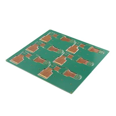
Let’s start with the basics: what “flatness” even means in PCB terms. For a Double Layers FR4 PCB, flatness refers to the deviation of the board’s surface from a perfectly flat plane when it’s lying free on a rigid surface—no external force applied, no bending to fit a case. FR4, a woven glass-reinforced epoxy laminate, is inherently prone to thermal expansion and contraction, especially after the high-temperature processes of lamination, solder masking, and assembly. That’s where most flatness issues come from, not a flaw in the design itself.
Now, the key part: the actual standard. If you’ve done any PCB research, you might have seen numbers like 0.75% or 1.5%, but let’s get specific. For mass-produced Double Layers FR4 PCBs (typically 0.4mm to 3.2mm thick, the range most electronics manufacturers use), the IPC-6012 specification is the gold standard. IPC, the Association Connecting Electronics Industries, sets performance standards for PCBs globally, and IPC-6012 breaks flatness into two main categories that matter for Double Layers FR4: Class 2 and Class 3.
Class 2 is for general electronic products—think consumer electronics, industrial control units, and most commercial devices. For Double Layers FR4 PCBs up to 1.6mm thick (the most popular thickness for smartphones, sensors, and power supplies), Class 2 flatness allows a maximum deviation of 0.75% of the board’s total length or width. Wait, let’s translate that to real measurements: a 100mm x 100mm Double Layers FR4 PCB would have a maximum allowed warp or curl of 0.75mm. For thicker boards, say 2.4mm, that threshold shifts slightly to 1.0% of the dimension, but that’s a caveat for later. Class 3, for high-reliability products like aerospace, medical devices, or automotive electronics, tightens that to 0.5% for boards under 1.6mm thick. That’s the sweet spot for our most demanding clients, and it’s what we focus on for critical assemblies.
But here’s what most suppliers won’t tell you: IPC-6012 is a baseline, not a one-size-fits-all rule. At our shop, we’ve worked with clients that need even tighter flatness—0.3% for PCBs used in high-frequency RF applications, where a tiny warp can throw off signal transmission. We don’t cut corners here, either. Testing flatness isn’t just eyeballing a board on a table; we use a Coordinate Measuring Machine (CMM) that scans the entire surface at 0.1mm increments to measure deviation, plus a portable flatness gauge for quick in-line checks during production.
Why does this matter to you, as a buyer? Let’s use a real example from a client we worked with last year: a small manufacturer of smart thermostats. They came to us after their previous supplier delivered Double Layers FR4 PCBs with 1.2% flatness deviation. Their pick-and-place machine, calibrated for Class 2 boards, kept misaligning SMD capacitors—12% of units got rejected mid-assembly, costing them $12,000 in rework and delayed shipments in the first month alone. We adjusted our lamination and post-curing processes to hit 0.6% flatness for their 1.2mm thick Double Layers FR4 boards, and their reject rate dropped to under 1%. That’s the difference between a standard and a custom-tuned solution.
Now, let’s break down what causes flatness issues in Double Layers FR4 PCBs, so you can avoid problems before they start. First is lamination: when we press the two layers of copper and FR4 together at 170°C, the epoxy resin flows unevenly, and if the press plates aren’t perfectly flat, the board can warp. Second is thermal cycling during assembly: when a PCB goes through a reflow oven at 260°C for solder, the FR4 expands, and when it cools, the layers shrink at slightly different rates. Third is storage: if PCBs are stacked too tightly or stored in humid conditions, FR4 can absorb moisture, leading to warping when heated later.
At our facility, we mitigate these issues with two key steps. First, a post-lamination flattening process where we place each Double Layers FR4 board on a precision ground steel plate and apply uniform pressure while heating it to 120°C. This eliminates residual stress from lamination before the board moves to routing and copper plating. Second, a 72-hour humidity-controlled storage period after manufacturing, so any moisture absorbed during handling evaporates slowly, no sudden expansion that causes warp.
But here’s a question we get all the time: what about thin Double Layers FR4 PCBs, under 0.8mm? The IPC standard still applies, but handling is trickier. Thin boards are more flexible, so even 0.5% flatness deviation can be enough to cause assembly issues. For these, we offer a temporary FR4 stiffener during pick-and-place, which is removed after assembly—another value-added service we’ve refined over the years.
Let’s address a common myth: some buyers think thicker boards are automatically flatter. Not true. We’ve produced 3.2mm thick Double Layers FR4 PCBs with 0.4% flatness deviation for a heavy-duty industrial power supply, because we controlled the lamination pressure evenly. Thickness matters, but process control matters more.
So, how can you verify that a supplier is actually meeting these flatness standards, instead of just saying they do? Ask for a flatness test report for a sample batch. A reputable supplier will provide CMM readings that show deviation across the entire board, not just a single corner. Also, ask about their post-manufacturing processes—if they skip the flattening step, that’s a red flag. At our shop, every Double Layers FR4 PCB gets a unique test sticker with a flatness reference number, so clients can cross-check against their own measurements if needed.
Another point: lead time doesn’t have to change for tight flatness requirements. A lot of buyers think, “If I need Class 3 flatness, I have to wait twice as long.” We’ve proven that wrong. Our standard turnaround for Double Layers FR4 PCBs is 5 to 7 business days, and we build flatness testing into that timeline, no extra delay. That’s why we’re preferred for clients who need both speed and quality for low-volume prototype runs and high-volume production.
Let’s wrap this up. The standard for Double Layers FR4 PCB flatness is rooted in IPC-6012, with Class 2 at 0.75% max deviation for most applications and Class 3 at 0.5% for high-reliability uses. But the true standard isn’t just the number—it’s a supplier’s ability to control processes from lamination to post-testing to deliver consistent flatness. As a supplier, we don’t just sell boards; we solve the problems that flatness causes on your assembly line.
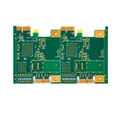
If you’re tired of dealing with Double Layers FR4 PCBs that warp, get rejected, or delay your production, get in touch with our team to discuss your specific requirements. We can provide sample boards, walk you through our testing process, and tailor a solution that fits your timeline and budget.
Double Layers FR4 PCB References:
IPC-6012: Qualification and Performance Specification for Rigid Printed Boards, Association Connecting Electronics Industries, 2022.
IPC-TM-650: Test Methods Manual, Section 2.4.22.1 Flatness Measurement, Association Connecting Electronics Industries, 2021.
Fastline Circuits Co., Limited
Fastline Circuits Co., Limited is one of the most professional double layers FR4 PCB manufacturers and suppliers in China. With abundant experience, we warmly welcome you to wholesale durable double layers FR4 PCB made in China here and get quotation from our factory. All customized products are with high quality and competitive price.
Address: Room 301, Building B3, Fuqiao 4th District, Qiaotou Community, Fuhai Subdistrict, Bao’an District, Shenzhen, Guangdong Province, China
E-mail: sales@fastlinepcb.com
WebSite: https://www.fastlinepcb.net/
